

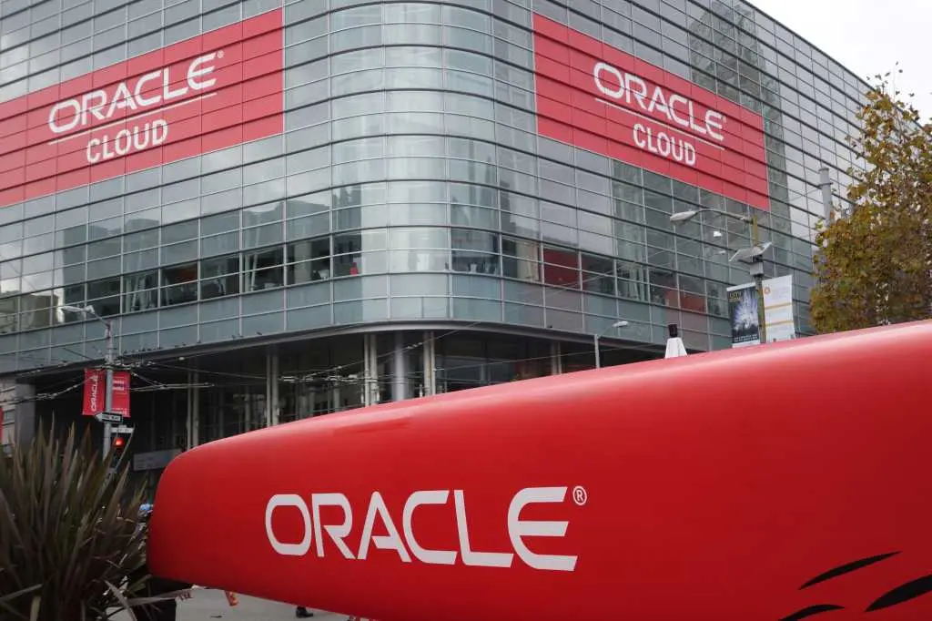
Oracle will offer Google's Tensor Processing Units through Oracle Cloud Infrastructure, giving enterprises a way to run training and inference workloads on Google-designed silicon without shifting those workloads onto Google's own cloud platform. The arrangement, announced at Oracle AI World in Las Vegas, marks the first time Google's TPUs have been made available through another hyperscaler, according to a joint statement from the two companies.
Under the agreement, Oracle supplies the data center infrastructure required to host the accelerators — power, cooling and networking — while Google supplies the chips themselves. Neither company disclosed which TPU generations would be deployed first, how the capacity would be priced, or how the OCI configurations would be structured for customers.
The only timing detail shared is that Oracle intends to make the chips available in calendar 2027, with capacity ramping up over multiple years. No specific launch date was given, and the companies did not say which regions would be served first or how customers would be able to reserve capacity ahead of general availability.
A first for Google's custom silicon
Google has spent more than a decade designing its own AI accelerators, a program that began as an internal effort to support machine learning workloads across its own services and eventually became a commercial product line sold to outside customers. Until now, accessing those chips at scale meant running workloads inside Google Cloud.
Extending TPUs into a rival hyperscaler's data centers represents a meaningful strategic shift. It positions Google's silicon as a component business that can compete on its own merits, separate from the cloud platform that surrounds it, and it gives Google a second channel into accounts that have standardized on a different primary cloud provider for regulatory, architectural or commercial reasons.
For Oracle, the deal broadens a compute portfolio that has been heavily oriented toward GPUs during the generative AI buildout. Enterprises that have committed to OCI for databases, applications and data gravity reasons now have an additional accelerator family to evaluate without re-platforming their surrounding infrastructure.
Why enterprises are looking past GPUs
The addition of TPUs expands the compute options available to Oracle customers as they search for alternatives to GPUs to manage the rising costs and infrastructure demands of training large AI models and running inference at scale, said Stephanie Walter, practice leader of AI stack at HyperFrame Research.
Inference workloads in particular stand to benefit, Walter noted, because they account for the largest share of compute consumption inside a typical enterprise. "Inference is a daily challenge," she said. "Every time an employee uses an AI assistant or an agent calls a model, it consumes compute."
That distinction matters because training is a finite, project-based expense, while inference is an ongoing operating cost that scales with adoption. As AI assistants, copilots and autonomous agents spread across an organization, the number of model calls grows continuously, and the cost per call becomes a line item that finance teams scrutinize.
Purpose-built accelerators such as TPUs can offer different performance and efficiency benefits depending on the model architecture, the workload and the software stack, Walter added, in contrast to GPUs, which are designed to handle a broader range of computing tasks. That flexibility cuts both ways: GPUs offer portability across frameworks and model families, while specialized silicon can deliver better economics when a workload maps cleanly onto its design.
What the eighth-generation TPU lineup offers
Google's TPUs are intended primarily for machine learning workloads, including large-model training, post-training and inference. The chips can also support reasoning-intensive and long-context applications, including those built around AI agents that make multiple model calls to complete a single task.
Google's eighth-generation TPU portfolio includes two distinct architectures. TPU 8t is designed for training and, according to the company, can deliver nearly three times the compute performance per pod of its predecessor while reducing frontier-model development cycles from months to weeks. TPU 8i is designed for inference, with an emphasis on the iterative workloads generated by multiple specialized AI agents operating in coordination.
The split reflects a broader industry pattern in which chip designers separate training and inference silicon rather than asking a single part to serve both phases efficiently. Training demands massive interconnect bandwidth and memory capacity to move gradients across thousands of chips, while inference is more sensitive to latency, throughput per watt and the cost of serving many small requests concurrently.
The switching-cost question
Access to the chips alone will not determine the economics of a deployment. Enterprises evaluating a new accelerator family must weigh the price of the hardware against the cost of adapting everything around it.
"An enterprise may have models, tools, and skills built around a different accelerator," Walter said. "Before switching, it needs to know what runs on TPUs, what needs to change, and how much effort it takes to maintain. A lower infrastructure price is not much of a bargain if the development and operational costs outweigh the savings."
Those costs are rarely trivial. Model code, serving frameworks, profiling tools, observability pipelines and the specialized expertise of platform engineers are typically tuned to a specific hardware target over many months. Compilers and runtime layers such as those used to run standard machine learning frameworks on TPUs add a layer of abstraction, but performance tuning still tends to be hardware-specific.
There is also the question of portability risk. Enterprises that concentrate their AI estate on a single accelerator family gain efficiency but expose themselves to supply constraints and pricing changes. Spreading workloads across multiple accelerator types reduces that exposure at the cost of operational complexity — a trade-off that many large organizations are only now beginning to confront as their AI spending matures.
A multi-cloud accelerator market takes shape
The arrangement fits a wider pattern in which cloud providers increasingly treat AI silicon as a portfolio decision rather than a single-vendor commitment. Hyperscalers have been building custom chips for training and inference, positioning them as cost-efficient complements to merchant GPUs, while also striking distribution agreements that place rival silicon inside their own data centers.
For enterprises, the practical effect is a market in which the same accelerator may be reachable from several providers, and where the deciding factors shift toward data locality, network architecture, contractual terms and the depth of managed services around the chip. Compute becomes one input among several rather than the entire basis for choosing a platform.
The timing also matters. AI infrastructure spending has climbed rapidly as organizations move experimental projects into production, and finance leaders are pressing technology teams to demonstrate unit economics for every workload they deploy. Purpose-built inference silicon is one of the few levers that can move cost per token without reducing model quality or cutting features.
What enterprises still cannot assess
The companies have not disclosed pricing, specific OCI configurations, or the initial capacity that will be available when the accelerators come online. Those details are likely to determine whether the additional accelerator option delivers meaningful cost or performance improvements for real workloads.
Capacity is a particularly sensitive variable. Announcing silicon availability and being able to fulfill orders at scale are different propositions, and enterprises planning multi-year AI roadmaps typically want committed capacity, predictable pricing and clear regional availability before they retool a production pipeline around a new chip family.
Until those details emerge, the announcement functions as a signal about direction rather than a procurement decision. It tells enterprises that OCI intends to compete on accelerator breadth, and it tells the market that Google's TPUs are moving toward a distribution model that does not require customers to adopt Google Cloud wholesale. Whether that translates into measurable adoption will depend on the specifications, the price per unit of throughput and the maturity of the software stack that surrounds the chips when they reach customer hands in 2027.
Source:Network World News